Premium FPGA Design-to-Deployment Expertise

Logitiles delivers high‑reliability, high‑performance and mission‑ready FPGA solutions built on more than two decades of hands‑on engineering experience. We support industrial, commercial and space‑grade organisations with robust architectures, deterministic performance and reproducible development flows.

RTL design is carried out in Verilog, VHDL or mixed‑language environments, depending on the customer’s toolchain, certification requirements and system architecture. This ensures full alignment with modern industrial practices as well as space/defense development standards.

Core Services

  • FPGA Architecture & RTL Design for complex, timing‑critical systems
  • High‑Speed Interfaces (SERDES, LVDS, PCIe, JESD204x and custom protocols)
  • Advanced DSP Pipelines for real‑time signal processing
  • Verification, Validation & Reproducible Design Flows
  • Deployment, Optimisation & Long‑Term Maintenance

Industries Served

  • Industrial automation & high‑reliability control systems
  • Commercial electronics & embedded platforms
  • Space & defense applications requiring mission‑critical robustness
  • Edge AI, sensor fusion & real‑time embedded computing

Why Logitiles

  • 20+ years of senior FPGA engineering experience
  • Design flows aligned with certification‑driven environments
  • Remote‑first workflow with transparent reporting
  • Risk‑reducing architecture, not commodity engineering
  • Long‑term reliability, maintainability and lifecycle support

It is important for all of us designers to know the device that will be used in the project, so that we can understand in advance if this component will be the most correct in terms of performance, production costs, market traceability, its behaviour in frequency, temperature or even with respect to ionising radiation (in the case of projects for devices in space).


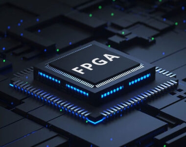
The first part helps the student understand what an FPGA is and what to expect from a component of this kind. This will be followed by a technological overview of the main blocks inside an FPGA up to their connection to the physical pins of the component. The main elementary logic cells of the main FPGA manufacturers will be illustrated, also trying to answer the following classic question: "what is the difference between LUT, LE, LC,...." so that it can then be possible for the student to understand whether a certain FPGA model of a manufacturer is more capacious or not (in terms of insertable logic) compared to a similar component of another manufacturer.


In the next few weeks we will announce the course calendar, the price of each course and any offers for multiple participation. For each course we will announce the list of topics and the duration of each one.

Cookies user preferences
We use cookies to ensure you to get the best experience on our website. If you decline the use of cookies, this website may not function as expected.
Accept all
Decline all
Analytics
Tools used to analyze the data to measure the effectiveness of a website and to understand how it works.
Google Analytics
Accept
Decline
Advertisement
If you accept, the ads on the page will be adapted to your preferences.
Google Ad
Accept
Decline
Save